Hybrid Phono Preamplifier MK I
The Concept
The full Circuit
Simulating the Circuit
Phono Preamplifier implemented
The Power Supply
Back to Main Page
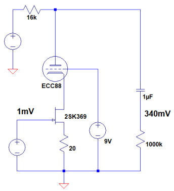
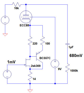
The Concept
This MC hybrid phono preamplifier was inspired by Allen Wright‘s elegant FVP designs (fig. 1a). The FVP input stage
comprises a jFet and a cascoding triode. The concept combines the high transconductance of the jFet and a high load
resistor value at the triode‘s plate resulting in a high gain input stage according to the equation
gain = gm
jFet
x R
Load
Furthermore cascoding the jFet keeps its drain voltage constant independent from the input signal and thus
eliminates the Miller effect. The Miller effect is nicely explained on this website. It may cause high dynamic input
capacitances of the jFets. A positive voltage at the grid elevates the cathode potential to ensure sufficient voltage at
the drain of the jFet. Allen‘s design includes a passive RIAA behind the input stage, two more amplifying triodes and a
sophisticated cathode follower at the output.
Drawback of an unbalanced cascode design is an almost 0db power source rejection ratio (PSRR). All „dirt“ on the
power supply +rail will appear at the plate of the cascoding triode due to its high impedance. Thus an extremely
clean power supply is needed when amplifying nano volt signals from MC cartridges. This is an even worse problem
in tube designs. Contrary to solid state circuits the mains transformer normally step up the power supply voltages
and with it all its noise, buzz, transients and voltage spikes.
Fig. 1a: Basic concept of Allen Wright‘s Fig. 1b: Basic concept of my own input Fig. 1c: Alternate concept for a high gain
FVP 5 input stage. Gain from the stage, already built and tested. input stage, so far simulated only
simulation is 51db.
Gain from the simulation is 57db. Gain from the simulation is 66db.
My own design tries to simplify Allen‘s concept while staying with the basic idea. The goal is a puristic unbalanced
preamp with a transistor based MC input plus one twin triode per channel only. The approach comprises a cascoding
input stage (fig. 1b) with very high gain followed by a passive RIAA and one more triode for further amplification as
shown in figure 2. Figure 1c shows an alternate input circuit with even higher gain. Momentarily it is just a conceptual
idea and is discussed in depth here. It has not jet been built while the circuit in figure 1b and figure 2 turned into a
fully operating phono stage that really performs nicely.
Back to top of the page
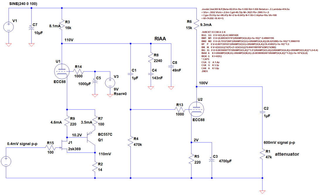
The full Circuit
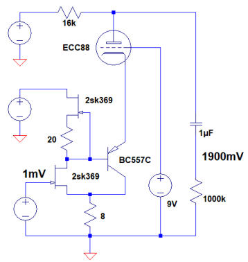
The input stage of the preamp comprises a 2SK369 njFet and a BC560C PNP BJT (BC557C in the simulation) in a
Sziklai configuration. R14 controls the idle current. R9 and R10 control the current distribution among the two
transistors. Both input transistors are cascoded by the first triode. The ECC88 is designed for cascode operation with
one specified triode for cascoding. A 9V battery at the grid of the first EC(C)88 elevates the cathode voltage to 11.2V.
Contrary to a voltage divider the chemically generated voltage from the battery is almost free from any noise. The
only battery load is the minuscule grid leakage current.
The input stage is followed by a passive RIAA and a second voltage amplifying triode at the output. For this design I
had to rule out MC step-up transformers. An input BJT would draw base current through the transformer coils which
hardly can be canceled out in an unbalanced design. With a jFET the input capacitance may become an obstacle. The
input capacitance of the 2SK369 jFet is 75pf. With a 1:8 step up transformer the reflected input capacitance would be
around 5.76nF.
C
in
= (step up ratio)
2
x (C
iss
+ C
rss
) = 5760pF
step up ratio = 8
C
iss
(2SK369) = 75pf
C
rss
(2SK369) = 15pf
Fig. 2: Schematic of the hybrid phono preamplifier. All currents and voltages are taken from LT SPICE simulation
The load resistor R3 as well as the grid resistor R4 are both RIAA critical. Details on the RIAA equalization network
design including a precision anti-RIAA circuit for SPICE simulation is described on the Laboratory Page of this web
site. The second (output) stage is a just a E(C)C88 in a plain common cathode configuration. The bypassing capacitor
C3 inhibits current feedback induced by the cathode resistor R5. Thus C3 increases the gain and lowers the output
impedance of the second stage. However, C3 might also be omitted if not needed.
R1 represents the attenuator. Potential limitations of the puristic design are
•
No protection of the MC cartridge from circuit failures at the input
•
An unbalanced input is more prone to pick up hum, buzz and noise
•
The power source rejection ratio is extremely poor
•
The ECC88 plate resistance is around 3kOhm. This limits the cable driving capability.
If the impedance of the output stage is not feasible the impedance converter from this website might be added to
drive long cables or critical loads.
Back to top of the page
Simulating the Circuit
All operating voltages and currents in figure 2 were derived from LT SPICE simulations of the circuit. Unfortunately
the total gain does not exactly meet low output MC requirements which would be around 0.4mV input voltage / 1V
output voltage @ 1kHz. With 0.4mV @1kHz at the input the output voltage is only 0.6V. However, this is sufficient for
medium or high output MC cartridges like the Benz Micro Wood (M).
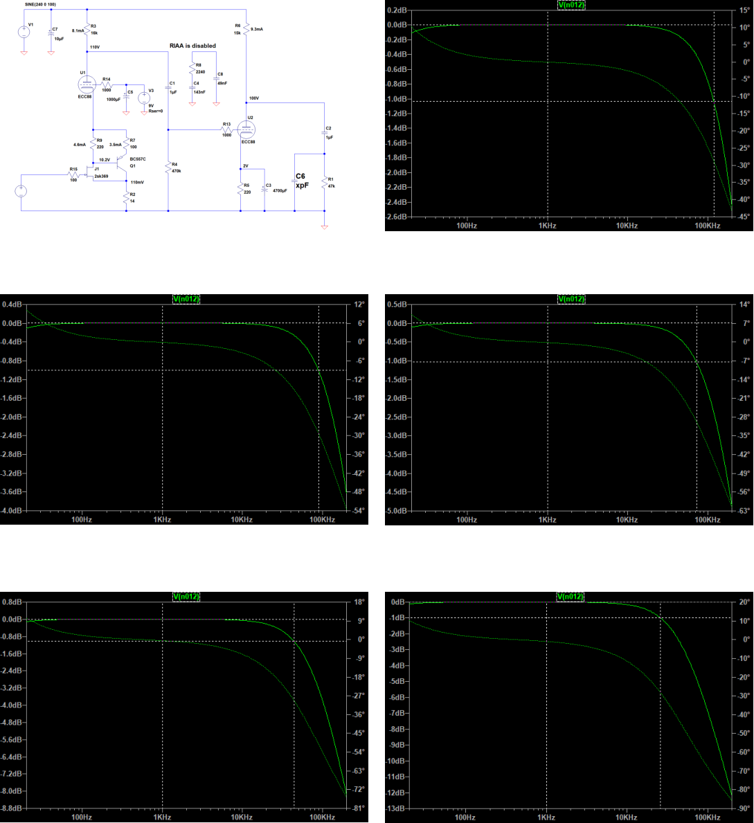
Capacitive Loads
As mentioned above the output impedance of the second stage roughly equals the plate resistance around 3kOhm.
Thus high cable capacitances will degrade the audio signal at high frequencies. Figure 3a shows the hybrid phono
stage with the RIAA disabled. The capacitor C6 in the schematic simulates different cable capacitances. The
simulations show the various -1db points at simulated cable capacitances of 100pF, 200pF, 500pF and 1000pF
(figures 3b to 3f). Typical cable capacitances are around 100pF to 300pF per meter (references: Audio Interconnect
Cables, Audio interconnect cables explained, Measuring the capacitance of some RCA cables). If we accept a high
frequency loss of -1db @ 45kHz (fig. 3e) an average audio interconnect cable should should be no longer than 2
meters.
Fig. 3a. Schematic of the hybrid phono stage. C6 simulates Fig. 3b: Frequency response of the circuit from figure 3a.
the cable capacitance. C6 = 0pF, The -1db point is @ 120kHz
Fig. 3c: Frequency response of the circuit from figure 3a. Fig. 3d: Frequency response of the circuit from figure 3a.
C6 = 100pF, The -1db point is @ 90kHz C6 = 200pF, The -1db point is @ 72kHz
Fig. 3e: Frequency response of the circuit from figure 3a. Fig. 3f: Frequency response of the circuit from figure 3a.
C6 = 500pF, The -1db point is @ 45kHz C6 = 1000pF, The -1db point is @ 26kHz
Back to top of the page
Phono preamplifier implemented
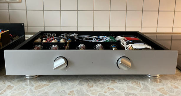
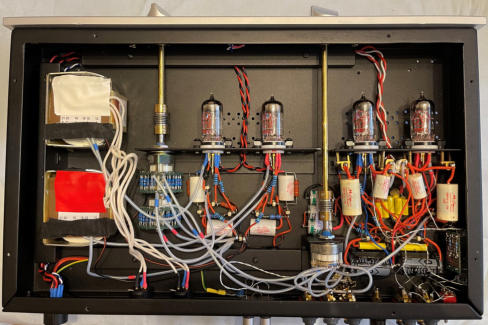
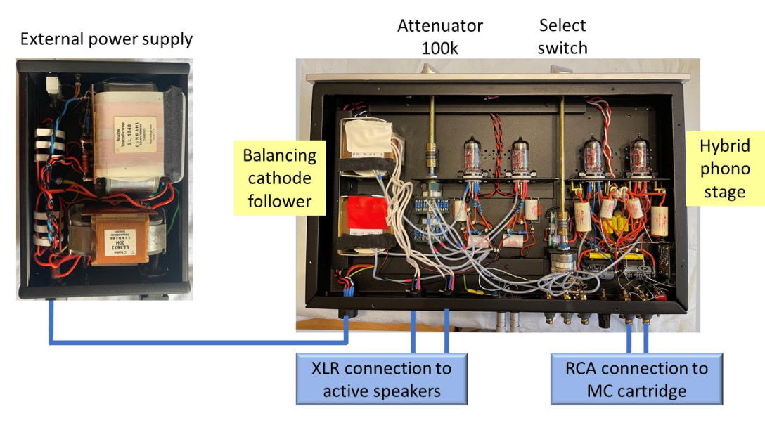
Figure 4 shows a simple block diagram of the phono preamplifier wired into the system. All electronic components
had to be fitted into two preexisting enclosures. Thus the wire routing is not at its optimum. The phono stage is
hooked up to a Benz Micro Wood (M). It provides a sufficient output voltage of 0.8mV. The balancing cathode
follower was added to drive active speakers with symmetric inputs and relatively low input impedances.
Fig. 4: Block diagram of the phono stage wired into the system.
Back to top of the page