Le Pacific Phono Preamplifier revisited
The modifications in this chapter have not been built.
They are just conceptual ideas.
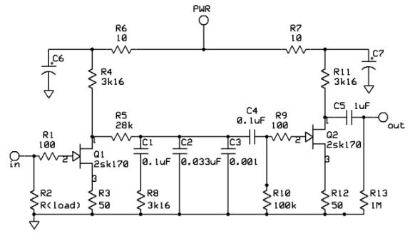
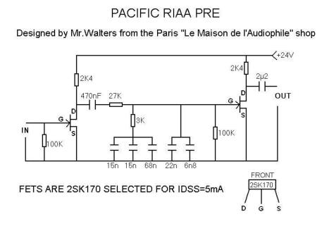
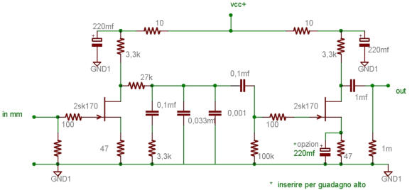
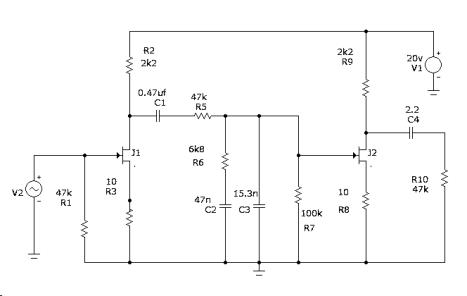
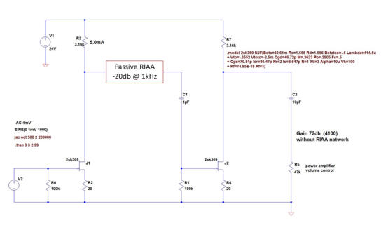
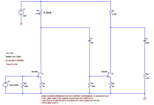
The Le Pacific phono preamplifier was introduced by Jean Hiraga. The circuit is based on two jFets and a passive RIAA
equalization in between (fig. 1). Its simplicity, cost effectiveness and safety made the Le Pacific preamplifier popular
in the DIY community. A number of schematic variants circulate on the internet, either with or without source
resistors, with the RIAA network in front or behind the first coupling capacitor, drain resistors vary between 2.2kOhm
and 3.3kOhm (fig. 2 to 4). 24V to 36V power supplies and low idle currents allow battery operation.
Fig. 1 to 4: Variants of the Le Pacific preamplifier (source Internet)
However, due to its somehow oversimplified design the Le Pacific phono preamplifier suffers from some inherent
shortcomings.
Low Gain
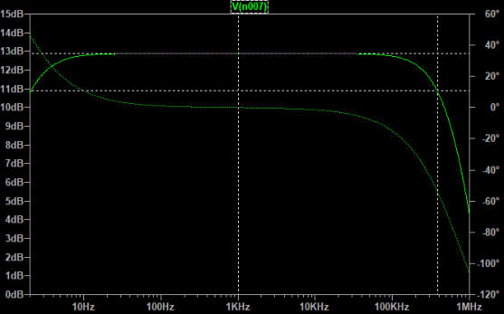
Figure 5 shows a SPICE simulation of the concept. For clarity the RIAA network is omitted from the circuit and only
the basic amplifying structure analyzed. The simulation in figure 5 reveals a gain of 62db. This is not impressive for @
1kHz the passive RIAA network will subtract 20db from the overall gain. This would be 500mV output voltage with
4mV at the input.
Fig. 5: Simulation if the original Le Pacific preamplifier with Fig. 6: Simulation with two 2SK369 jFets instead of the 2SK170.
2SK170 jFets (RIAA omitted). Gain is 62db. Gain is 72db.
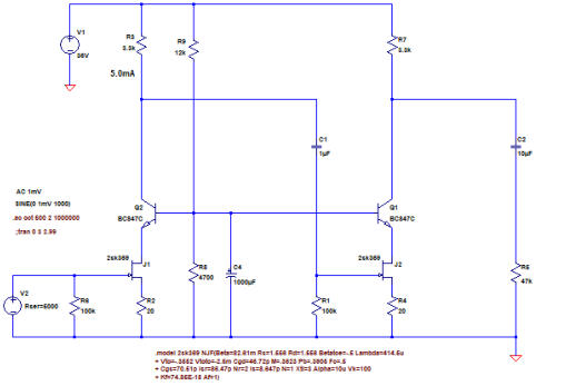
To increase gain the degeneration source resistors may be omitted and the jFets selected for idle currents of 5mA @
Vgs=0 as in the design by Walters (fig. 2). Drawback is a positive Vgs with the input signals. The gate may draw
current and the input impedance may be compromised. A better solution might be jFets with higher transcon-
ductance such as the 2Sk369. The 2SK369 requires a source resistor around 20Ohm to settle the idle currents at 5mA
(fig. 6). The source resistors also ensure stability and some local feedback. The SPICE simulation in figure 6 reveals a
gain of 72db. With 20db subtracted from the passive RIAA 4mV input voltage would reveal 1.6V at the output.
Limited Bandwidth
A fundamental problem of the Le Pacific concept is the limited bandwidth due to the Miller effect of the input
transistor. The Miller effect is nicely explained on this website. It causes a high dynamic input capacitance Cin of the
jFets. Cin is derived from the following equation:
Cin = Cgs + Cgd x (A+1) (Miller capacitance)
Cin = input capacitance
Cgs = gate-to-source capacitance
Cgd = gate-to-drain capacitance
A = stage gain (first stage in figure 5 or 6)
For the simulation in figure 6 (2SK369) the calculated input capacitance Cin is
Cin = 75pF + 15pF x (70 + 1) = 1140pF
An input capacitance of 1.14nF is far above the recommended capacitive load for MM cartridges. Even with the
2SK170 as input transistor Cin is still quite high. According to the data sheet and the simulation in figure 5 Cin of the
first 2SK170 is
Cin = 30pF + 6pF x (36 + 1) = 252pF
Increasing Bandwidth by Cascoding the jFets
Cascoding the jFets with two BJTs will eliminate this problem. The BJTs keep the voltage at the jFet drains constant
and the variable A in the above equations becomes 1. Figures 7 and 8 show SPICE simulations of the original Le
Pacific design and a cascoded design, both with 2SK369 jFets. Power supply voltage is set to 36V, because an
additional 9V to 10V are needed for the cascoding transistors. The impedance of the input voltage source is set to
5kOhm to simulate high impedance MM cartridges. Figures 7b and 8b show the frequency responses.
Fig. 7a. Le Pacific layout with 2SK369 jFet Fig. 7b: Frequency response of the circuit from figure 7a
Fig. 8a. cascoded Le Pacific layout with 2SK369 jFet Fig. 8b: Frequency response of the circuit from figure 8a
With reference to 1kHz the conventional design shows a -3db roll-off @20kHz (fig. 7b) while the cascoded design
looses 0.006db @20kHz. Its -2db roll-off is beyond 350kHz in the simulation (fig. 8b). The modification to a cascoded
design will need few more components. It is safe and simple. Costs are minuscule.
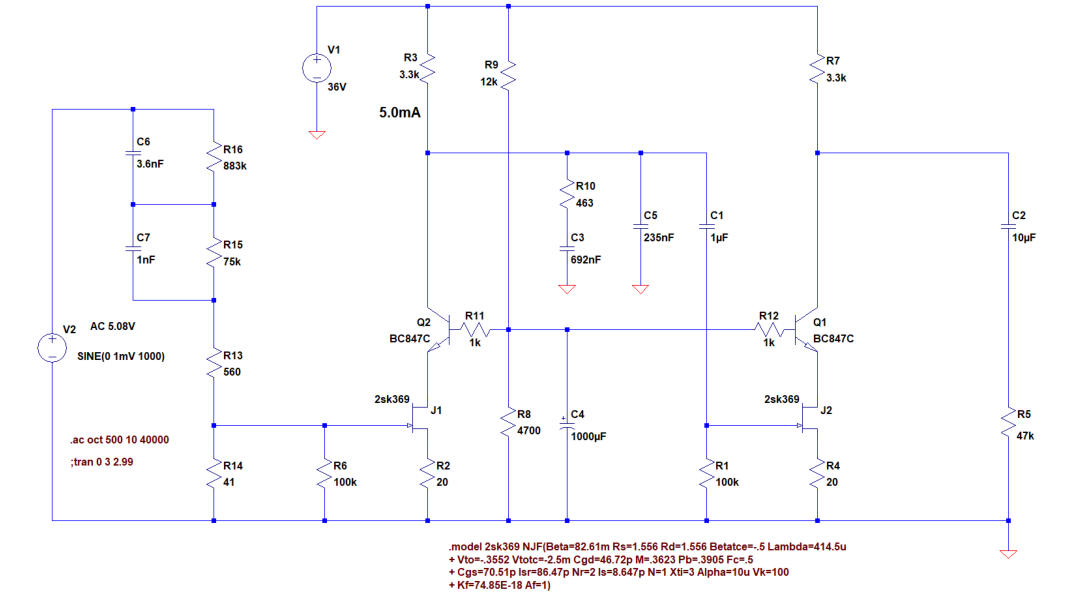
Modified RIAA Network
A cascode is an almost perfect current source. This allows the use of a so called transconductance RIAA. The network
comprising R1, R3, R10, C3 and C5 in figure 9 resembles a variable load which is fed from the current source Q2.
With rising frequency the network impedance decreases and the voltage drop at R3 corresponds with the RIAA curve.
Main advantage is the omission of the series resistor in the conventional passive RIAA network. Figure 9 shows the
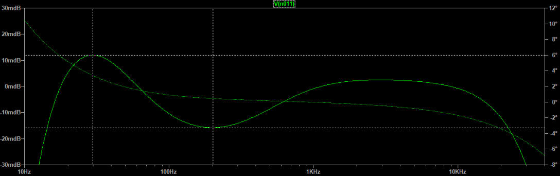
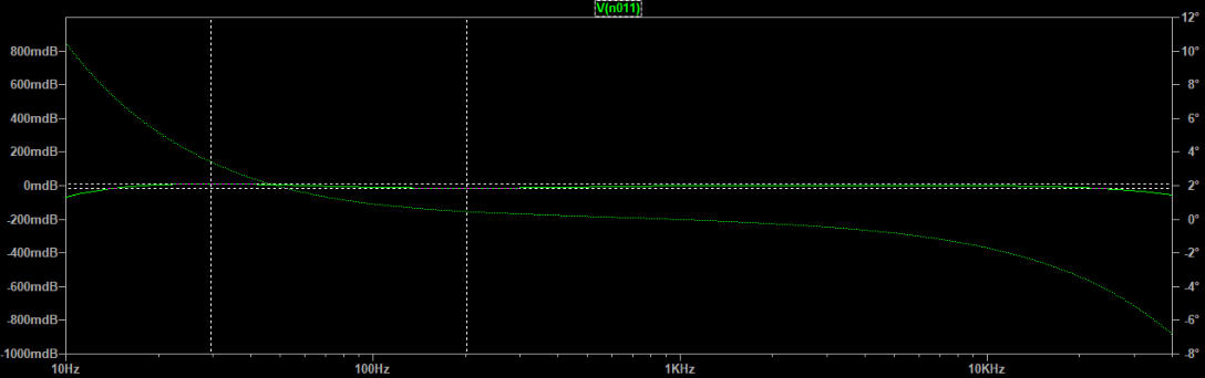
cascoded circuit with the recalculated RIAA network. The input signal is fed through a precise anti-RIAA filter. Thus
the frequency response at the output must be flat. As shown in figure 10 and 11 the the diversion from the ideal
RIAA is within a range of 30mdb. Further information on the anti-RIAA filter can be found here.
Fig. 9: Circuit diagram with transconductance RIAA network and anti-RIAA filter at the input.
Fig. 10: Frequency response with anti-RIAA filter at the input. The scale is +/- 1db on the ordinate axis.
Fig. 11: Frequency response with anti-RIAA filter at the input. The scale is +/- 30mdb on the ordinate axis..
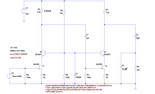
Output Impedance
The different Le Pacific designs from figure 1 to 4 as well as the modifications only can drive short cables for the
output impedance roughly equals that of the drain resistors or collector resistors respectively. Thus higher cable
capacitances will degrade the high frequency response of the circuit. Figure 12a again shows the cascoded Le Pacific
layout with 2SK369 jFets from the above figure 8. The capacitor C4 in the schematic simulates different cable
capacitances. The simulations show the various upper -1db points @ simulated cable capacitances of 100pF, 200pF,
500pF and 1000pF (figures 12b to 12f).
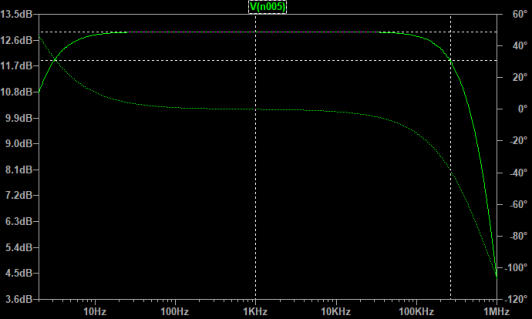
Fig. 12a. cascoded Le Pacific with simulated cable capacitance Fig. 12b: Frequency response with cable capacitance = 0pF.
-1db point is at 260 kHz
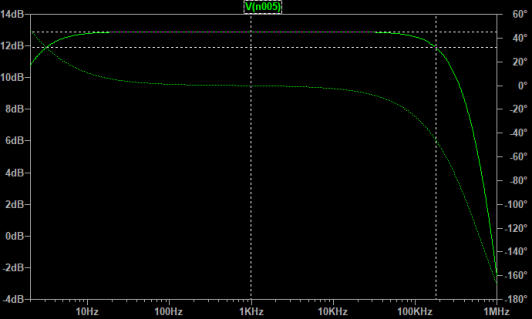
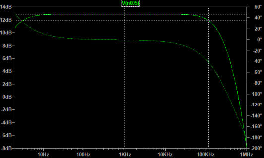
Fig. 12c: Frequency response with cable capacitance = 100pF. Fig. 12d: Frequency response with cable capacitance = 200pF.
-1db point is at 180 kHz
-1db point is at 115 kHz
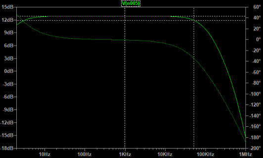
Fig. 12e: Frequency response with cable capacitance = 500pF. Fig. 12f: Frequency response with cable capacitance = 1000pF.
-1db point is at 50 kHz
-1db point is at 25 kHz
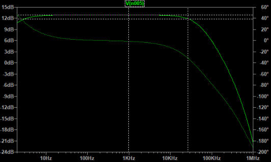
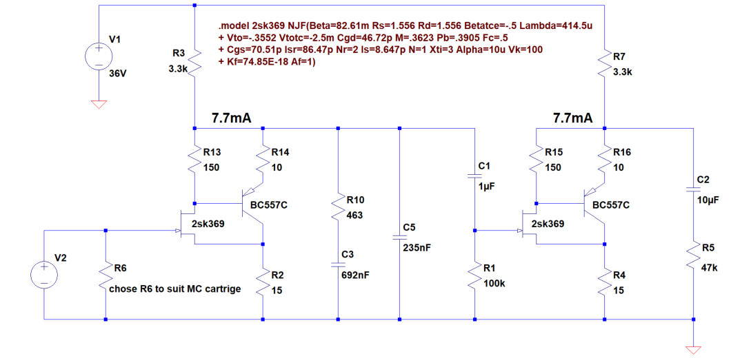
Enhancing the Gain to MC Level
Figure 13 below shows a simple modification to elevate the gain to full MC level. Each stage comprises an additional
BC560 (BC557C in the simulation) PNP low noise transistor connected to the 2SK369 jFet in a Sziklai configuration.
The two resistors of 10Ohm and 150Ohm split the idle currents to 4.5mA for the jFet and 3.2mA for the bipolar
transistor. The total idle is 7.7mA. The cascode configuration mentioned above has been discarded. Due to the low
input impedances of most MC cartriges the input capacitance of the first j-Fet will hardly compromise bandwidth and
thus might be neglected. Ignoring the RIAA network the gain of each stage is 44db. With an input voltage of 0.4mV
the circuit (with RIAA network) delivers around 1.2V at the output.
Fig. 13: Modified circuit of the Le Pacific phono preamplifier for MC cartriges.